Challenges in Electronics Packaging
A guide to electronics packaging. This abstract covers key challenges like thermal management, material selection, sustainability, and future trends in miniaturization.
Summary
Challenges in Electronics Packaging refers to the complex issues faced in the design, production, and implementation of protective casings and frameworks for electronic components. As technology advances, the demand for efficient, reliable, and sustainable electronics packaging has intensified, making it a critical area within the broader field of engineering. Notably, the evolution of electronic devices toward miniaturization and increased functionality has heightened the importance of effective packaging solutions, which are essential for maintaining device performance, reliability, and user satisfaction.
The primary challenges in electronics packaging encompass thermal management, material selection, regulatory compliance, heterogeneous integration, and sustainability. Effective thermal management is crucial as the miniaturization of components leads to increased heat generation, necessitating innovative cooling techniques to prevent performance degradation and failure. Additionally, the selection of appropriate materials is vital to protect sensitive components from environmental factors while ensuring electrical insulation and thermal conductivity. Compliance with stringent regulations, such as the Restriction of Hazardous Substances (RoHS) directive, poses further complexity for manufacturers aiming to innovate while adhering to legal standards.
Emerging trends in the industry reflect a growing commitment to sustainability, with companies exploring biodegradable materials and eco-friendly designs. The shift towards more integrated packaging solutions, including 2.5D and 3D architectures, has transformed the landscape of electronics packaging by enabling enhanced performance and reduced space requirements. However, the balancing act between achieving sustainability goals and maintaining product performance remains a contentious issue among industry stakeholders.
Overall, the field of electronics packaging is at a critical juncture, driven by rapid technological advancements and shifting market demands. The ongoing challenges and innovations in this domain highlight its significance not only in ensuring the functionality of electronic devices but also in addressing broader environmental concerns and regulatory requirements, making it a notable area of study within engineering and technology disciplines.
Table of Contents
Historical Background
The history of electronics packaging can be traced back to the nineteenth century, when materials such as steel, aluminum, and polymers began to be utilized for electric and electronic enclosures. As technology progressed, the evolution of electronics packaging closely followed advancements in semiconductor technology and the miniaturization of electronic components. Key milestones in this evolution include the introduction of dual in-line packages (DIPs) in the 1960s, which revolutionized the way electronic components were housed, and the emergence of surface-mount technology (SMT) in the 1980s, which allowed for more compact and efficient designs.
In recent years, the development of packaging has been further driven by the demand for 3D packaging and system-in-package (SiP) solutions, which address the increasing complexity and integration of electronic devices. This evolution reflects a growing recognition of the critical role that packaging plays not only in protecting sensitive components but also in ensuring optimal performance within increasingly compact electronic systems.
Over time, the considerations for electronics packaging have expanded to include various factors such as mechanical, thermal, electrical, and environmental considerations. The integration of advanced materials and manufacturing processes has become essential in addressing the thermal challenges posed by modern electronics. Additionally, the rise of consumer electronics and the subsequent demand for reliable packaging solutions have further fueled innovation and evolution in this field, making it a significant discipline within mechanical engineering.
Types of Electronics Packaging
Electronics packaging encompasses a variety of techniques and materials tailored to protect and enhance the performance of electronic components and systems. This section categorizes the different types of packaging based on structure, materials, and application, reflecting the evolution and innovation in the field.
Levels of Packaging
The packaging of electronic systems can be organized into several hierarchical levels, each addressing specific requirements for protection and functionality: Level 0 – Chip: This level focuses on protecting a bare semiconductor die from contamination and physical damage. Level 1 – Component: At this level, packaging involves semiconductor package design and the assembly of discrete components. Level 2 – Etched Wiring Board: This includes printed circuit boards (PCBs), which connect and mechanically support components. Level 3 – Assembly: Comprises one or more wiring boards along with their associated components. Level 4 – Module: Involves integrated assemblies enclosed within a single structure. Level 5 – System: Represents a complete set of modules combined to serve a specific purpose, such as a portable device or a fixed installation in an instrument rack or other permanent locations.
Traditional Packaging Materials
The selection of materials is crucial in electronics packaging, affecting the reliability, cost, and performance of the final product. Plastics: Widely used due to their low cost, ease of processing, and versatility. Types include epoxy, polyimide, and polycarbonate. Metals: Essential for providing thermal conductivity and electrical shielding, with common examples being copper, aluminum, and gold. Ceramics: Known for their high thermal conductivity, electrical insulation, and resistance to harsh environments, with materials such as alumina (Al2O3), silicon carbide (SiC), and aluminum nitride (AIN) being prevalent.
Advanced Packaging Technologies
As semiconductor technology evolves, new packaging techniques have emerged to meet the demand for compact and high-performance devices: 2.5D Packaging: This method uses an interposer to connect multiple chips horizontally, enhancing communication speed and reducing latency while maintaining manageable manufacturing complexity. 3D Packaging: Involves stacking chips vertically and connecting them with through-silicon vias (TSVs), which minimizes signal path lengths and boosts performance, particularly in applications requiring high speed and power efficiency, such as AI accelerators and data centers.
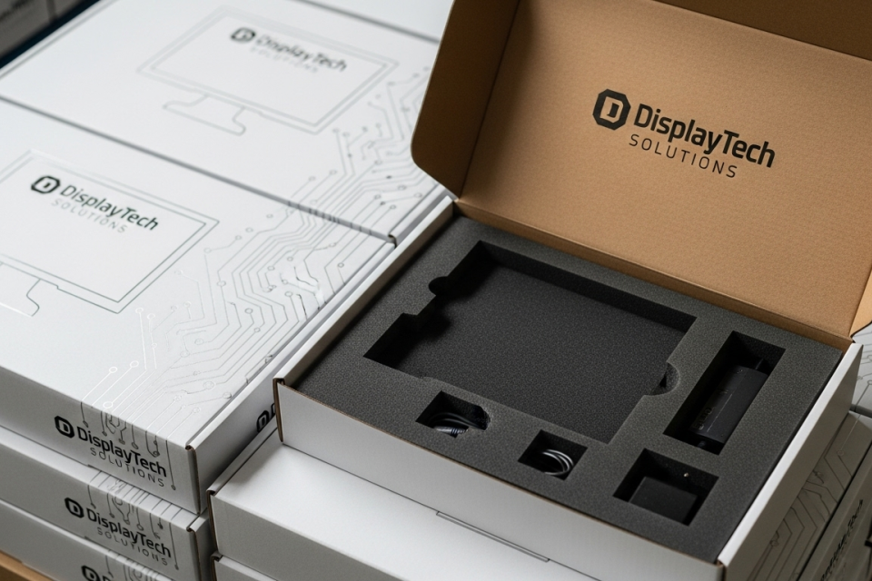
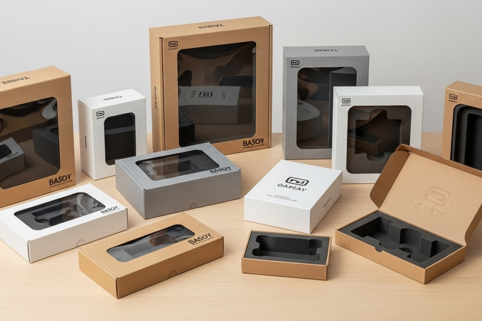
Specialized Packaging for Consumer Electronics
Consumer electronics require packaging that not only protects the components but also appeals to the user. Product Protection: Ensuring that fragile electrical components are shielded from damage during handling and transport, particularly as online shopping grows. Visual Appeal: Enhancing the perceived value of the product through attractive packaging designs. User Experience: Designing packaging that is easy to open and convenient for the user while being optimized for efficient shipping.
Emerging Trends
The industry is witnessing a trend toward sustainability, with packaging companies developing biodegradable materials and optimizing processes to reduce waste and carbon emissions. Innovations such as fan-out wafer-level packaging (FOWLP) further exemplify the drive for miniaturization and enhanced electrical performance, particularly in compact electronic devices like smartphones and wearables.

Key Challenges in Electronics Packaging
Electronics packaging faces several critical challenges that affect the performance, reliability, and sustainability of electronic devices. These challenges arise from the need to protect sensitive components, manage heat dissipation, and comply with regulatory standards.
Thermal Management
Effective thermal management is crucial for maintaining the performance and reliability of electronic devices. As electronic components become smaller and more powerful, managing heat generation and dissipation becomes increasingly complex. High power densities can lead to significant heat accumulation, which, if not adequately managed, can degrade component efficacy and reliability. Various thermal management techniques, including natural and forced convection cooling, are employed to address these issues, but the choice of solution often depends on the specific application and design constraints.
Material Selection
The selection of appropriate materials for packaging is another significant challenge. Packaging materials must provide adequate protection from environmental factors while also facilitating heat transfer and ensuring electrical insulation. The development of new materials, such as advanced thermal interface materials (TIMs), aims to improve thermal conductivity and performance without compromising other properties. However, balancing performance with sustainability is a growing concern, as manufacturers face pressure to adopt eco-friendly materials while still meeting technical requirements.
Regulatory Compliance
Electronics packaging must adhere to various regulatory standards, such as the Restriction of Hazardous Substances (RoHS) and the Waste Electrical and Electronic Equipment (WEEE) directives. Compliance with these regulations requires careful consideration during the design and manufacturing processes to limit hazardous materials and ensure proper disposal of electronic waste. Navigating these regulations can complicate the packaging design process, especially for companies looking to innovate while adhering to legal requirements.
Heterogeneous Integration
The trend towards heterogeneous integration, where different types of components are packaged together, presents unique challenges in electronics packaging. This integration demands advanced design techniques to effectively manage thermal paths and minimize the risk of overheating, as closely packed components can exacerbate heat dissipation issues. As electronic designs evolve towards 2.5D and 3D integrated circuits, ensuring reliable thermal management becomes even more critical to avoid potential damage from thermal stresses.
Sustainability Concerns
With the increasing focus on sustainability, the electronics packaging industry faces challenges in adopting new, environmentally friendly materials without sacrificing performance. Manufacturers must strike a balance between sustainability and functionality, exploring innovative solutions that promote a circular economy while meeting the demanding requirements of modern electronics. The transition to sustainable packaging materials is further complicated by the need to maintain competitive costs and performance levels.

Innovations in Electronics Packaging
Advancements in Materials
The landscape of electronics packaging is rapidly evolving, primarily driven by the integration of advanced materials that enhance performance and support miniaturization. Key innovations include the development of composites, nanomaterials, and smart materials. Composites, such as carbon fiber reinforced polymers (CFRP) and metal matrix composites (MMC), provide tailored properties that improve mechanical strength and thermal management. Nanomaterials like carbon nanotubes (CNTs) and graphene offer unique characteristics due to their nanoscale structure, contributing to enhanced electrical conductivity and thermal performance. Additionally, smart materials that react to external stimuli, such as shape-memory alloys (SMAs) and piezoelectric materials, are increasingly being explored for dynamic and responsive packaging solutions.
Miniaturization and Functionality
The trend towards miniaturization is a significant driver of innovation in electronics packaging. As devices become smaller, the demand for packaging solutions that maintain or improve functionality while reducing size is paramount. Innovations in this area focus on achieving enhanced performance, increased portability, and cost reductions. The rise of IoT-connected devices, smartphones, and wearables has further accelerated this trend, necessitating packaging solutions that protect delicate components during transport and use. Moreover, advancements in 3D printing technology are enabling more complex geometries and designs, allowing for greater flexibility in packaging solutions.
Sustainability Initiatives
Sustainability is becoming a critical aspect of innovation in electronics packaging. The exploration of durable, non-scratch, and recyclable materials aims to minimize environmental impact while ensuring product longevity. The adoption of biodegradable materials is also gaining traction, as they are designed to decompose naturally over time, thus reducing pollution and enhancing sustainability. This shift towards eco-friendly materials reflects a growing recognition of the need for sustainable practices within the electronics industry.
Emerging Technologies
The integration of advanced technologies is playing a crucial role in shaping the future of electronics packaging. The advent of 5G, autonomous vehicles, and artificial intelligence (AI) is driving the demand for advanced packaging solutions that can meet the complex requirements of these applications. Furthermore, the rise of the Internet of Things (IoT) within the packaging industry enables real-time monitoring and control, enhancing traceability and efficiency. Innovations in thermal management materials, such as carbonaceous materials and advanced composites, are providing significant improvements in thermal conductivity, allowing for the elimination of traditional cooling systems, thereby enhancing overall system reliability.

Future Trends in Electronics Packaging
Innovations in Materials and Sustainability
The future of electronics packaging is increasingly focused on sustainability, with a significant push towards the use of durable, non-scratch, and recyclable materials. This trend is driven by the need for environmentally conscious practices, as tech companies work to reduce plastic usage and enhance recyclability in their packaging solutions. Major manufacturers, like Apple, have committed to eliminating plastic from all packaging by 2025, transitioning towards fiber-based designs that align with their sustainability goals. Furthermore, the electronics industry is looking to develop flexible and stretchable semiconductor packaging materials, enabling new applications in wearable technology and smart textiles.
Miniaturization and Advanced Technologies
As electronic components continue to shrink, the trend towards miniaturization in packaging is expected to accelerate. This evolution allows for the integration of more functions into smaller packages, leading to the development of compact and powerful devices such as medical implants and Internet of Things (IoT) sensors. Advanced technologies such as 3D packaging and system-in-package (SiP) solutions are at the forefront of this trend, offering improved performance while minimizing physical dimensions. The integration of through-silicon vias (TSVs) in 3D packaging enhances power efficiency and overall performance, making it a key area of focus for future developments.
Adoption of AI and Automation
Artificial intelligence (AI) and machine learning are expected to play a critical role in the future of electronics packaging. These technologies can optimize layout designs, material selection, and manufacturing processes, thereby reducing development cycles and improving yield rates. Additionally, automation in packaging processes is anticipated to enhance efficiency, lower labor costs, and minimize material waste, aligning with the industry’s push for sustainability. The convergence of AI and packaging technology not only accelerates innovation but also improves the time-to-market for new products.
Regulatory Challenges and Market Adaptability
While the electronics packaging market is evolving rapidly, it faces regulatory challenges related to packaging materials and waste disposal. Global standards are continually changing, which necessitates that manufacturers adapt their packaging solutions to comply with new regulations. Moreover, the increased sale of consumer electronics through e-commerce has raised the demand for secure and appealing packaging that protects products while enhancing brand image. This need for adaptability underscores the importance of regular packaging audits and the implementation of customized packaging solutions that minimize material usage and costs.
Logistics and Cost Management Challenges
Logistics costs in the electronics packaging sector are multifaceted and critical for maintaining supply chain efficiency. These expenses can be categorized into several key components, including transportation, inventory, and labor costs, which collectively impact the overall profitability of companies operating in this field.
Transportation Costs
Transportation is a significant part of logistics expenses, as it involves the movement of goods from manufacturers to consumers. This includes various fees such as fuel charges, tolls, and shipping rates that fluctuate based on distance and mode of transport. Ensuring timely delivery while controlling these costs remains a major challenge for businesses in the electronics sector, particularly in an environment marked by rising customer demand and labor shortages.
Inventory Management
Inventory costs also pose a challenge, as they encompass expenses related to warehousing and stock management. This includes rental fees for storage facilities, insurance against potential loss or damage, and costs associated with maintaining software systems for inventory tracking. Furthermore, the proper management of inventory is crucial, given that many consumer electronics consist of numerous components that must be effectively stored and organized to optimize space and reduce waste.
Labor Costs
Labor represents another significant expense in logistics operations. The wages, benefits, and training costs associated with staff vary depending on the location and skill level required for specific tasks. Companies must navigate the complexities of labor availability and associated costs, especially in regions experiencing workforce shortages.
Technological and Global Challenges
The landscape of logistics is further complicated by technological advancements and global challenges, including geopolitical tensions and climate-related issues. These factors necessitate a shift from traditional supply chain processes to more innovative solutions that leverage data and technology for better decision-making. Companies are increasingly adopting AI and analytics-driven management approaches to enhance forecasting accuracy and procurement efficiency, which are vital for mitigating disruptions and managing costs effectively.